


Virtual Conference: Semicon Meets Sustainability
November 5, 2024 | 8:00 a.m. CET and 5:00 p.m. CET
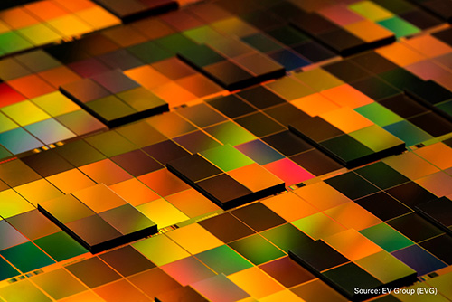
Reducing Energy Consumption Through Smart Back-End Packaging and Innovative Materials
The virtual conference "Semicon Meets Sustainability" is brought to you by DELO and will be held on Tuesday, November 5, 2024, from 8:00 a.m.–10:15 a.m. CET and in a condensed format from 5:00 p.m. – 6:40 p.m. CET.
It will feature presentations from semiconductor experts discussing trends and the latest developments in sustainable back-end packaging. In addition, smart materials and technologies for photonics integration that can help reduce energy consumption in the future when processing AI-generated data will be highlighted.
You are warmly invited to ask any specific questions after each presentation.
If you work in semiconductor back-end packaging and are interested in learning more on how to employ sustainable practices, this virtual conference is for you.
Want to join us? Registrations are now open on Microsoft Teams Webinar. The deadline to sign up is November 5, 2024, 6:00 a.m. CET, two hours before conference start. The conference will be held in English language.
We are looking forward to welcoming you at our virtual conference this November.
Register now for free!
WITH EXPERTS FROM:
PRESENTED BY:
PROGRAM
Welcome and Keynote: Technological Progress and Reduced Energy Consumption: Two Sides of the Same Coin?
8:00 a.m. – 8:15 a.m. | Dr. Tobias Königer (Keynote) & Markus Willemeit (Moderation), DELO
A world without microchips is no longer conceivable. They are key to our connected world, with AI, self-driving cars, and wearables that monitor our health. However, semiconductor manufacturing is one of the world’s most energy-intensive production processes, mainly attributed to front-end, but also with back-end packaging playing an integral role. On top of this, the processing of data generated by advanced technologies will drive energy demand to a new high in the years to come. So, the question is: Are we facing two sides of the same coin, or can we have both technological progress and an environment with less carbon emissions?
Reinforcement Reimagined: Disruptive Technologies for Sustainability
8:15 a.m. – 8:30 a.m. | Robert Hofmockel, DELO
When bringing sustainability and semiconductors together, it’s hard not to think about durability and the importance of conserving resources during production. This presentation will highlight leading edge reinforcement technologies such as UV Snap-Cure Edge Bond, one-step Corner Fill and Activation on the Flow. These technologies can increase the durability of components and help reduce carbon emissions. You will get technical insights and a deep dive into advanced solutions that are critical to the future of sustainable semiconductors.

A Holistic Approach for Chiplet Packaging
8:30 a.m. – 8:45 a.m. | Karl-Friedrich Becker, Fraunhofer IZM
Innovative packaging solutions play a crucial role in modern electronics manufacturing. A promising technology that can help reduce a product’s ecological footprint are chiplets. These small integrated circuits can be used in lieu of large monolithic chips and be combined in a modular way. In this presentation we will talk about this advanced packaging technology, including chiplet encapsulation and chiplet module assembly. We will also show how these systems can improve resource effiency and contribute to the vision of a greener, more environmentally friendly society.
Saving Energy in Fan-Out Packaging
8:45 a.m. – 9:00 a.m. | Dr. Markus Schindler, DELO
In Fan-Out Wafer/Panel-Level Packaging, warpage after molding poses a severe limitation in handling and heightening of RDL resolution. UV-curable large-area encapsulation materials can overcome warpage and offer a sub-micron die shift. These will be the focus of this presentation. The use of UV light for curing instead of energy-intensive ovens for heat curing is a promising solution that offers technological advantages while contributing to a more sustainable room-temperature process.
Wafer Carrier and Maskless Patterning Solution for Multi-Functional Chiplets in Advanced System-in-Package (SiP)
9:00 a.m. – 9:15 a.m. | Dr. Thomas Uhrmann, EVG
The heterogeneous integration of chiplets is one challenge within the fast-growing advanced packaging industry, especially since carrier technologies and lithographic patterning capabilities are determinative technologies crucial for advanced system-in-package designs. This is particularly challenging in large-die interposer fabrications, where stitch-lines and or mismatches overlap regions within the reticle exposure field can affect the RDL’s electrical properties. The ability to generate a stitchless pattern for interposers exceeding current reticle size is important for advanced devices needed for complex layouts, such as advanced graphic processing, AI and high-performance computing (HPC). In this presentation, you will get insights into maskless pattering solutions as an environmently-friendly option.
Future Outlook: Advanced Semiconductor Packaging in HPC and Photonics Integration
9:15 a.m. – 9:30 a.m. | Dr. Shababa Selim, IDTechEx
In our quest for a greener future, utilizing advanced semiconductor packaging technologies for optical integration in high-speed data communication can significantly enhance energy efficiency and reduce environmental impact from data centers and communication networks. This integration can lead to faster data transfer rates, lower power consumption, and a reduced carbon footprint, making it a key component in building a more sustainable and eco-friendly technological infrastructure.
In this presentation, IDTechEx will disucss its recent research findings in the field of advanced semiconductor packaging including the trends, drivers, and challenges of this industry. Also, an outlook on future developments in key application sectors will be provided, focusing on HPC chips and the incorporation of optical/photonics technology through advanced semiconductor packaging.
Adhesives for Silicon Photonics / Photonic Integrated Circuits (PIC)
9:30 a.m. – 9:45 a.m. | Oliver Matyssek, DELO
With much discussion within the industry, Photonic Integrated Circuits (PIC) are shaping up to be the future of optical communication technology. They require reliable adhesives for uses such as optical and edge coupling as well as v-groove bonding. This presentation will provide you with an overview of the optical and mechanical properties of newly developed materials. Experiments conducted by DELO, together with external partners like iNemi, Tyndall or Sabic, underscore the coupling efficiency of such optical bonds. You will also get insights into recent advancements in adhesive technology and how these will contribute to the development of more efficient and reliable photonic devices.

Optical-in-Package Solution with 3rd Generation of FOPLP
9:45 a.m. – 10:00 a.m. | Steve Jin, OIP Technology
With its third generation of Fan-Out Panel Level Packaging (FOPLP) OIP Technology is at the forefront of developing advanced optical products with a focus on high-growth markets such as AI, automotive, and mobile applications. It is a key innovation in optical and electronic device integration. This integration reduces power consumption and enhances the bandwidth between electronic devices. The presentation will showcase the advantages of optical integrated products for FOPLP in comparison to traditional semiconductor packages. One of that is the substrate-free design, making them ideal for high-frequency applications like silicon photonics, laser oscillators, and high-power charging products.
Conclusion of Event
10.00 a.m. – 10:15 a.m | Moderator
The virtual conference will be closed with a short recap. There will also be time again for your specific questions and discussion.
Register now and become inspired
WITH EXPERTS FROM:


Meet DELO’s Semicon Specialists
SEMICON Europa 2024 | November 12 - 15 | Messe München (Germany)
Booth C2740 / hall C2
Take this chance to talk on site about sustainable solutions for advanced packaging as well as your specific bonding challenges.